透過第一原理計算來研究1T-HfSe2以及1T-PtSe2過渡金屬二硫族化物(transition metal dichalcogenides)的結構、電子、以及傳輸特性;我們更進一步解釋為何這兩種化合物具有相同的1T (八面體)層狀結構,但卻存在非常不同的電子和傳輸特性。我們發現有兩個決定性的因素(i)過度金屬的5d價電子數以及(ii)層內鍵結離子性。因此,我們認為1T-HfSe2所具有的二維傳輸特性,以及在1T-PtSe2中可透過層數所調控的金屬-半導體轉換,可以應用在新型態的奈米電子以及光電元件開發。
In this study, we employed the first-principles calculation to investigate the structural, electronic and transport properties of 1T-HfSe2 and 1T-PtSe2 transition metal dichalcogenides, and further explain why they share the same 1T (octahedral) layered structure but exhibit very different electronic and transport properties. There are two underlying concepts: the degree of intralayer bond ionicity and the number of 5d valence electrons of transition metal. The high degree of Hf-Se bond ionicity not only gives rise to the indirect energy gap of HfSe2 bulk and thin films, but also results in the weak Se-Se vdW interlayer coupling to further restrict the electron transport only within a HfSe2 layer. On the other hand, the modulation of metallic/semiconducting property of PtSe2 bulk and thin films can be understood by the significant vdW interlayer coupling, which induces charge redistribution of Se atom and allows electrons to transport within a PtSe2 layer as well as cross neighboring layers. Finally, our transport calculation for 1T-HfSe2/1T-PtSe2 bulks and monolayers suggests the great electron transport within Hf-Se/Pt-Se layer but suppresses/allows electron from neighboring layers. The robust two-dimensional characteristic of 1T-HfSe2 and the metal-to-semiconductor transition of 1T-PtSe2 may provide more knowledge for future application in nanoelectronic and optoelectronic devices.
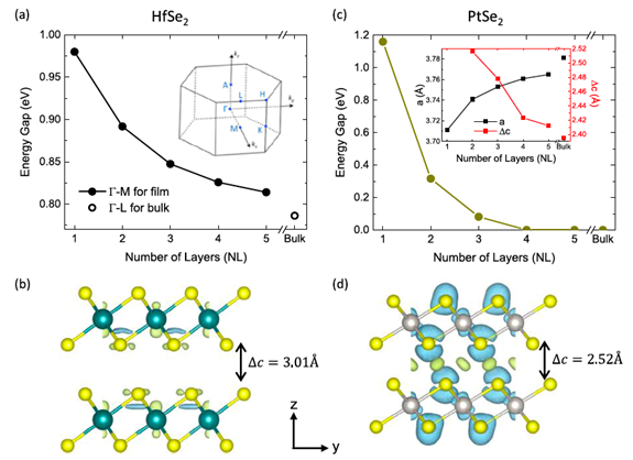
(a) Energy gap evolution for the indirect energy gap of (a) 1T-HfSe2 (Γ-L for bulk and Γ-M for NL thin films). (b) Differential charge density with the isosurfaces of ± 0.0002 e/Bohr3 (yellow/blue) for 1T-HfSe2 between 2L and 1L films. (c) Energy gap evolution for the metal-semiconductor transition of 1T-PtSe2. The inset shows layer dependence of lattice constant, a, [left-hand coordinate] and of vdW interlayer distance, Δc, [right-hand coordinate]. (d) Differential charge density with the isosurfaces of ± 0.0007 e/Bohr3 (yellow/blue) for 1T-PtSe2 between 2L and 1L films.